Rising Relevance of Two Inch Indium Phosphide Wafers in Quantum Research and Prototype Development
The Global Indium Phosphide Wafer Market is projected to exhibit steady and structured growth from 2023 to 2032, with demand primarily driven by the larger diameter categories that underpin high-performance photonic devices, optical communication modules, and advanced sensing technologies. Data indicates that the 100 mm (four inches and above) category maintains the strongest position throughout the forecast period. This segment is expected to increase from $200.08 million in 2023 to $534.08 million by 2032, reflecting a compound annual growth rate of 12.09% from 2025 to 2032. This sustained growth trajectory is indicative of a widespread industry shift toward higher efficiency manufacturing processes, alongside the rising deployment of next-generation photonic integrated circuits that necessitate stable, defect-controlled, and larger format wafers for mass production. The adoption of photonic chips in high-speed transceivers, data centers, long-haul networks, and cloud infrastructure significantly supports the dominance of this segment. Furthermore, larger wafers contribute to reducing overall fabrication costs per device by allowing more dies to be processed in a single run, aligning well with the global trend toward cost-optimized production of optical components. This category is bolstered by ongoing investments from major players who are expanding their capabilities for larger diameter indium phosphide substrates in response to increasing orders from telecom and datacom vendors.
The 76.2 mm (three inches) segment remains a vital middle-tier category, with its value projected to grow from $120.01 million in 2023 to $254.15 million in 2032, achieving a compound annual growth rate of 8.77% during the forecast period. Despite a lower growth rate compared to the larger diameter category, this segment demonstrates consistent and stable utilization across various sectors, including aerospace, defense, industrial measurement, and specialty optoelectronic applications.
Manufacturers and research units often prefer this size due to established fabrication lines, predictable yield performance, and strong compatibility with various epitaxial techniques utilized in photonics and sensor development. This wafer size is frequently adopted by organizations focused on precision devices, such as narrow linewidth lasers, optical amplifiers, advanced detectors, and high-reliability components for military systems. Its continued presence in the market underscores the operational and economic value of maintaining production for medium-diameter substrates that cater to a wide array of mid-volume and high-stability applications, even as industry leaders transition to larger wafers.
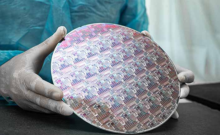
The 50.8 mm (two inches) segment is anticipated to grow from $39.84 million in 2023 to $88.84 million in 2032, reflecting a compound annual growth rate of 9.55%. This segment serves specialized and small-scale manufacturing environments, including academic research centers, prototype development laboratories, niche device manufacturers, and early-stage photonics innovators. Although it accounts for the smallest share of the total market, its growth rate highlights its sustained significance in low-volume sectors, where precision, controlled defect densities, and flexible processing are prioritized over production scale. This segment also supports experimental testing of new materials, new epitaxial structures, quantum photonics experiments, and compact sensor designs that may require limited quantities but demand high-quality substrate characteristics. Many breakthrough technologies in photonics commence with this diameter before scaling up to larger wafer formats after successful validation.
Overall, the indium phosphide wafer market is set to expand from $359.92 million in 2023 to $877.07 million by 2032, with a compound annual growth rate of 10.79% from 2025 onward. This growth is attributed to a combination of commercial scale expansion, increasing global communication needs, and the diversification of photonic applications across multiple industries. The rising adoption of high-speed networks, cloud computing, artificial intelligence-driven data centers, and ultrafast communication systems is driving demand for components manufactured from indium phosphide. These include lasers, modulators, detectors, and integrated photonic circuits, which are essential for modern digital infrastructure. Indium phosphide is favored for its superior electron mobility and direct bandgap properties, making it the material of choice for high-frequency and optical devices where performance is critical.
Additionally, the automotive sector is progressively adopting indium phosphide-based lidar systems and advanced sensing modules to enhance safety and autonomous driving capabilities. The medical sector also plays a role through the use of indium phosphide devices in imaging systems and diagnostic tools. Furthermore, defense and aerospace programs require reliable photonic components for advanced communication links, ranging systems, secure channels, and surveillance systems. Each of these sectors contributes to the increasing demand for wafers across all diameter categories.